

ICS1000EL Solar Panel Inspector
Overview
Electroluminescence is the emission of photons from a solar cell under an applied forward bias.
Measuring the photographic electroluminescence of a photovoltaic device provides valuable spatially-resolved details about efficiency-degrading mechanisms in the cell, array, or panel.
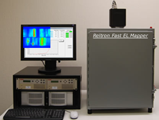
The Reltron Fast EL Mapper is an integrated solution designed specifically for solar applications to provide both quantitative and relative values of various parameters of the device for all configurations: cells, strings, and large-area panels.
Applications
- Process control/QA
- Research and Development
- Inline manufacturing
- Sorting and grading
Measurements
- Minority carrier lifetime (diffusion length)
- Micro cracks
- Lateral Series Resistance
- Shunt Resistance
- Defects and impurities in the semiconductor
- Open circuits or discontinuities in conductors
- Polysilicon grain boundaries
- Relative efficiency
Standard Features
- High rez Enhanced-NIR Sensor with >1.4MPixels and binning capability; TEC cooled.
- 16-bit Pixel Depth and 32-bit Signal Processing for unsurpassed precision
- NIR-optimized optics customized for your application and field of view
- Built-in 4-quadrant IV curve tracer with up to 1KW output power
- Photovoltaic device sizes from 6mmX6mm cells up to 2.3X2.6 meter modules
- High Power USB-controlled 660nm and 1064nm Illuminators
- Custom designed light-tight Dark Box per your device size requirements
- 19in Rack mounted PC and curve tracer power supplies
- Photovoltaic Imaging Software Suite running on Windows XP Pro/Vista/Win7
Optional Features
- Motorized Camera Sensor focus
- Motorized Camera Sensor X-Y stage
- Higher resolution sensor (up to 16Mpixel)
- 640x480 InGaAs Camera Sensor
ICS1000EL Fast EL Mapper Image Gallery
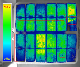
6inx6in polySi solar array EL overlay with various defects: cracks, increased series resistance areas, puncture, and regions of reduced minority carrier lifetime
EL closeup of puncture and polysilicon grain boundaries. Can you tell the difference between boundaries and a micro crack? Reltron can!
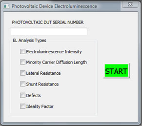
Reltron Photovoltaic Imaging Suite provides not just images, but also performs analysis on the photovoltaic DUT
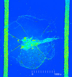
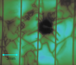
Closeup of crack; spacing between conductors is 3mm. Note 1068um scale on image
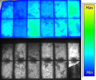
Monochrome image is raw EL. Color image on top is measured relative minority carrier diffusion length. Note that the dark areas along the center of the array on lower image do not impact carrier diffusion, indicating that these are areas of higher lateral resistance